| Group members: | M. Morales Masis, E. Rucavado, R. Monnard, G. Charitat. A. Hessler-Wyser, Q. Jeangros, F. Landucci |
| Running projects: | Swiss National Science Foundation (SNFS), Swiss Commission for Technology and Innovation (CTI) and Competence Center Energy and Mobility (CCEM) |
Keywords: transparent electrodes, metal oxides, tin, zinc and indium oxide, amorphous TCOs, materials design, solar cells, OLEDs
Background
In the transparent conducting oxide (TCO) group we are working on the understanding and development of TCO materials and its applications. We use a combination of fundamental physics and material studies, conventional thin film deposition, combinatorial growth and characterization techniques, to develop TCO films that will match the specific application requirements in solar cells and other novel optoelectronic devices. Our TCO thin films are currently being used as electrodes for silicon heterojunction solar cells, perovskite/silicon tandem solar cells and organic light emitting diodes (OLEDs).
Research highlights
High mobility TCOs for high-efficiency solar cells
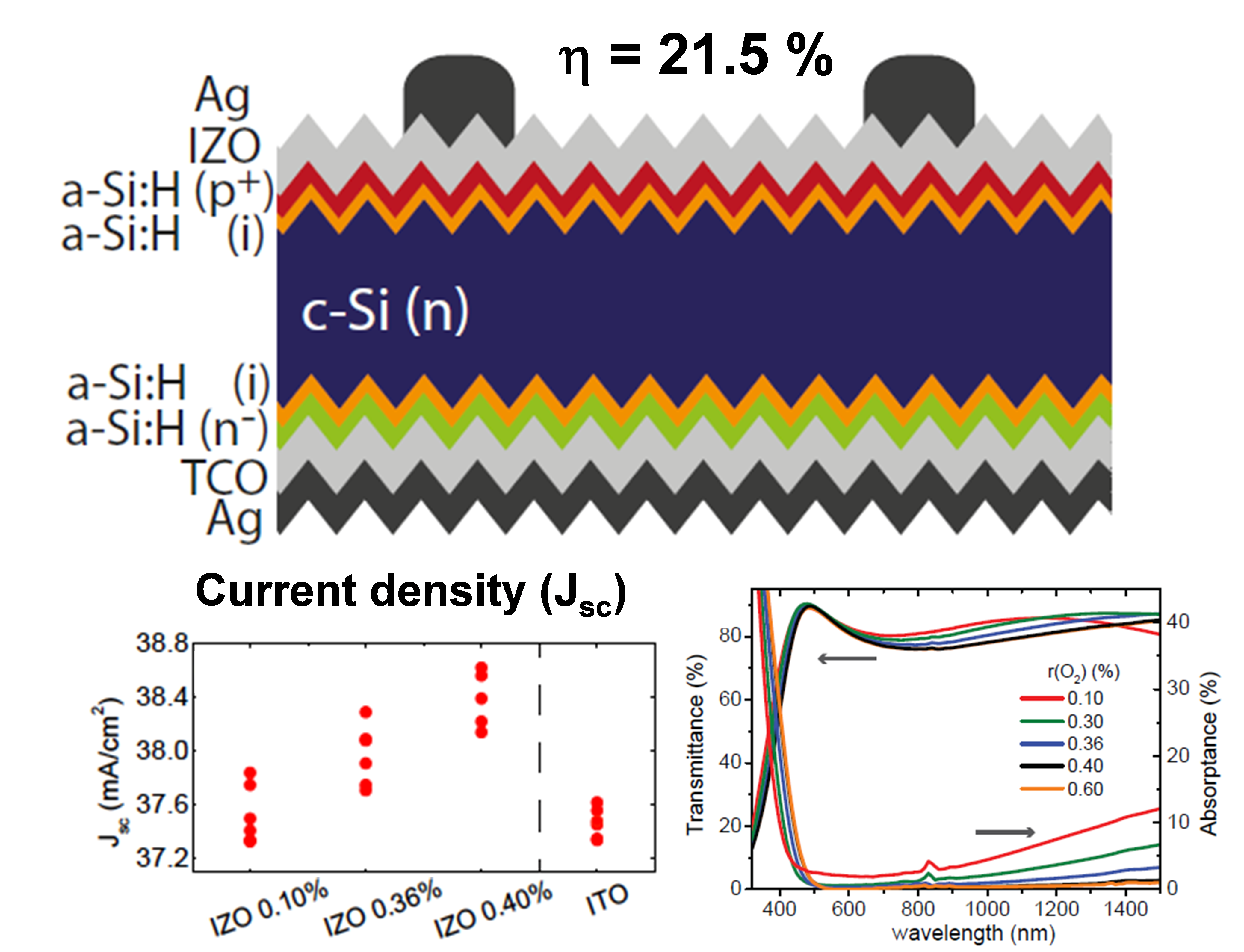 Solar cells such as silicon heterojunction (SHJ) solar cells (Fig.1) and perovskite-on-silicon tandem solar cells, as well as new designs like bifacial and semitransparent solar cells, employ TCOs in their designs. At the front of the solar cells, these TCO layers act as the optically transparent electrode that allows photons into the solar cell and transports the photo-generated electrons to the external device terminals. Therefore, high lateral conductivity and low UV-IR absorption are crucial requirements of the front TCO of any solar cell device. To avoid parasitic optical losses in the NIR-IR, TCO’s with high electron mobility instead of high free carrier densities are required. Following this, we have developed and studied high mobility TCOs such as indium zinc oxide (IZO), hydrogenated indium oxide (IO:H), zirconium doped indium oxide (In2O3:Zr), and selectively apply them in SHJ (Ref. 2 and 9) and perovskite solar cells (Ref. 2). The cells with high mobility TCOs show an improvement in conversion efficiencies, due to higher current densities (Jsc) as compared to reference ITO, while keeping the required low contact resistance with the adjacent layers.
Material design of indium-free TCOs
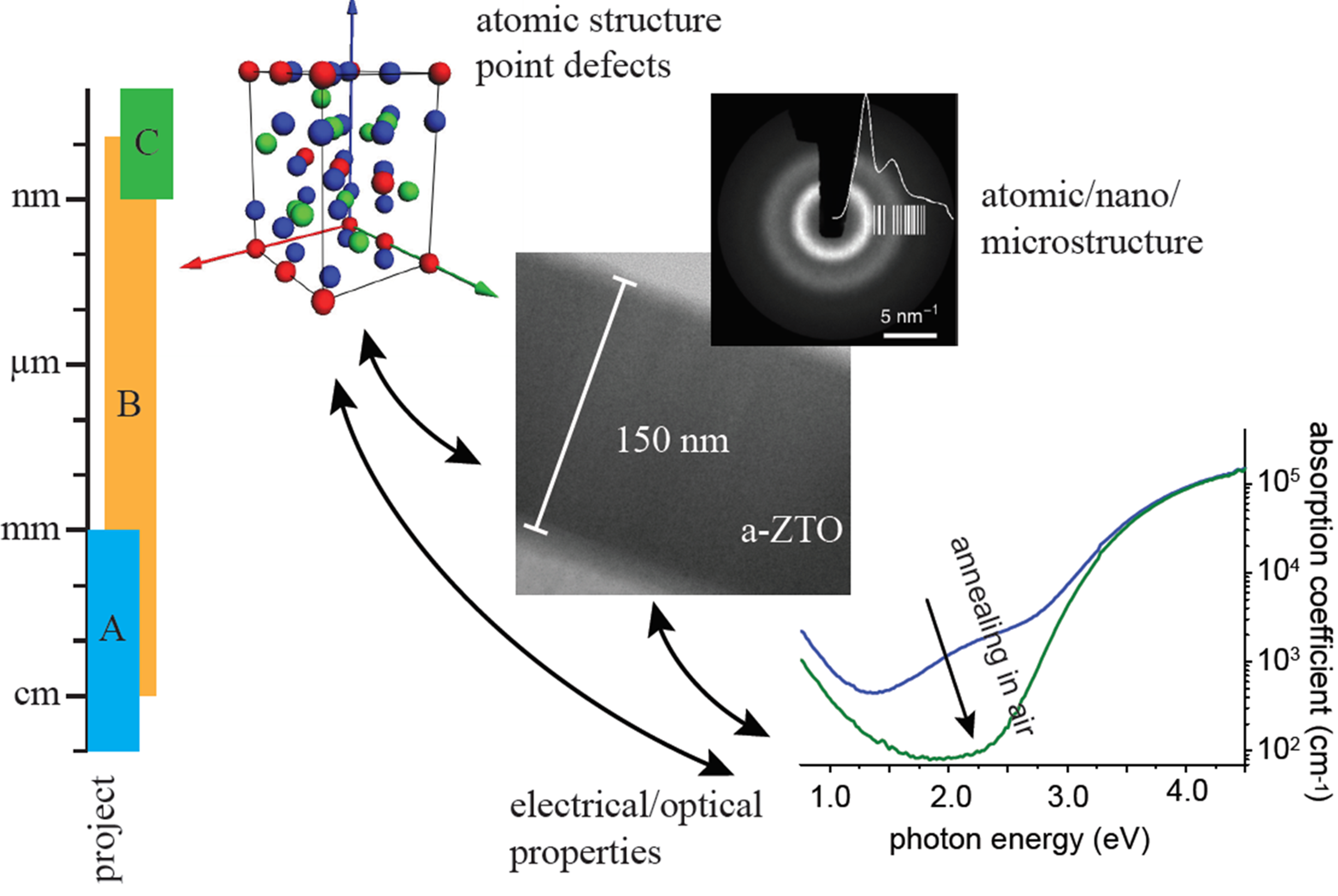 The design of new high-performance indium-free TCOs, remains an important task to reduce costs in several optoelectronic devices. Following an interdisciplinary approach, we are working on the development and understanding of multi-compound indium-free TCOs. Recently, we have demonstrated a remarkable improvement of the optoelectronic properties of zinc tin oxide (ZTO) by the passivation of sub-gap atomic-scale defects. In close collaboration with computational and advanced microscopy groups, we have identified the nature of these defects, and their role with respect to the electron mobility and optical properties (Ref. 1). Transmission electron microscopy (TEM) studies furthermore revealed that the ZTO films have an amorphous and dense microstructure, which remains stable up to 500 °C, making this material highly interesting for applications requiring high-temperature treatments (Ref. 4).
Indium-free anodes for OLEDs
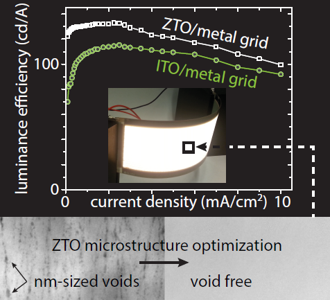 By combinatorial screening of ZnO and SnO2 compounds using co-sputtering deposition, we have developed a zinc tin oxide (ZTO) anode for large-area flexible OLEDs (Ref. 6). The anodes are fabricated at low temperatures for compatibility with plastic flexible substrates. Optimization of the sputtering parameters leads to the growth of a dense amorphous microstructure with optimized electron mobilities up to 22 cm2/Vs, and less than 5% absorptance in the visible range of the spectra. The amorphous ZTO anodes present higher mechanical stability to bending and stretching as compared to other polycrystalline TCOs, as demonstrated in Ref. 5.
Low Pressure Chemical Vapor Deposition (LPCVD) of ZnO:B
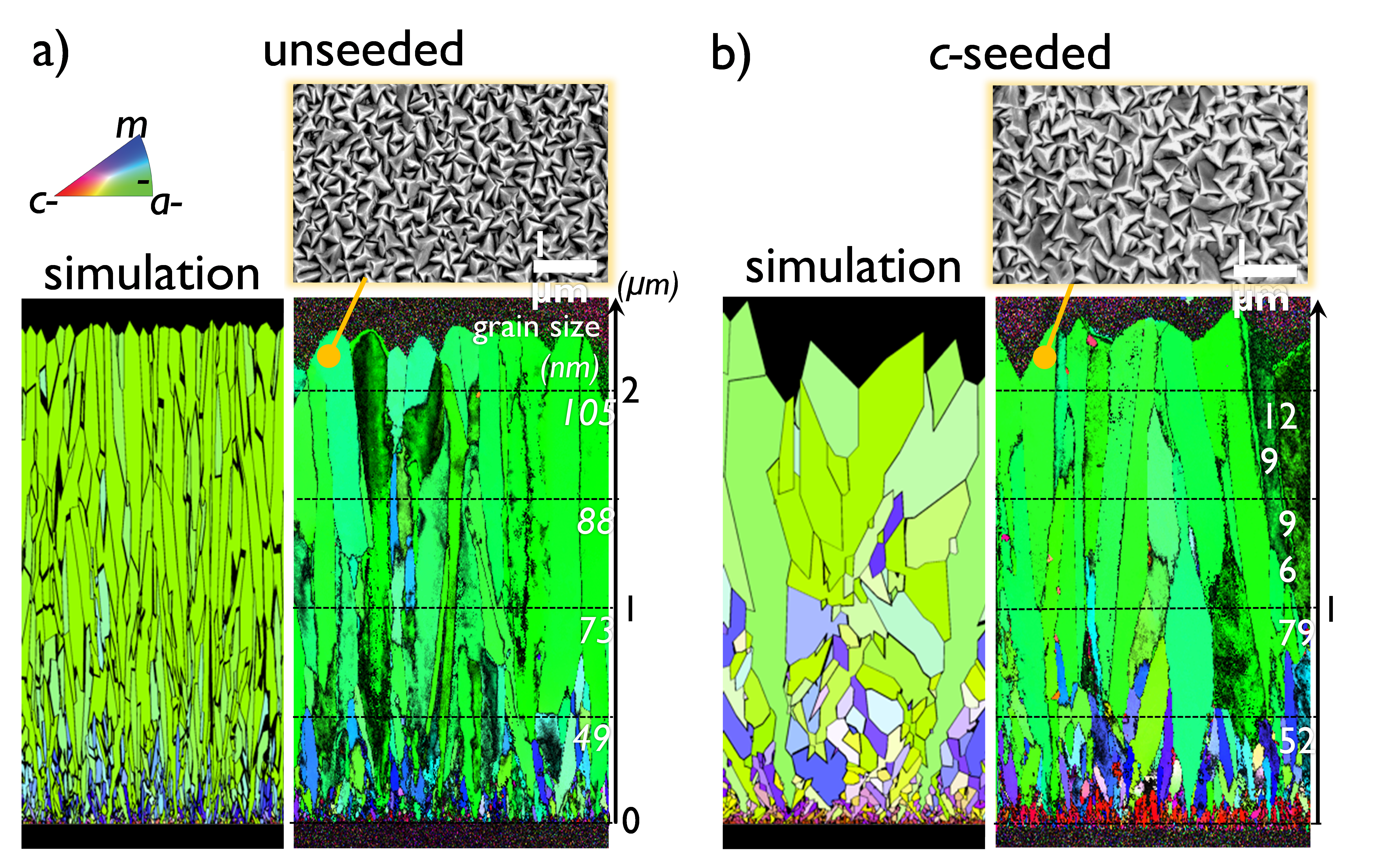 Low-pressure chemical vapor deposition (LPCVD) is a highly versatile technique to grow highly transparent and conductive zinc oxide (ZnO) films with distinct surface morphologies. The final morphology of the films is controlled by variations in the growth parameters, going from rough pyramid-like surfaces -widely used for light scattering in thin films solar cells-, to smooth surfaces and even porous films. In addition, we have demonstrated the controlled tuning of the ZnO grain sizes by selecting the seed layer. Increasing the grain size resulted in improved electron mobility typically limited by grain boundary scattering (Fig. a and b. Ref. 11).
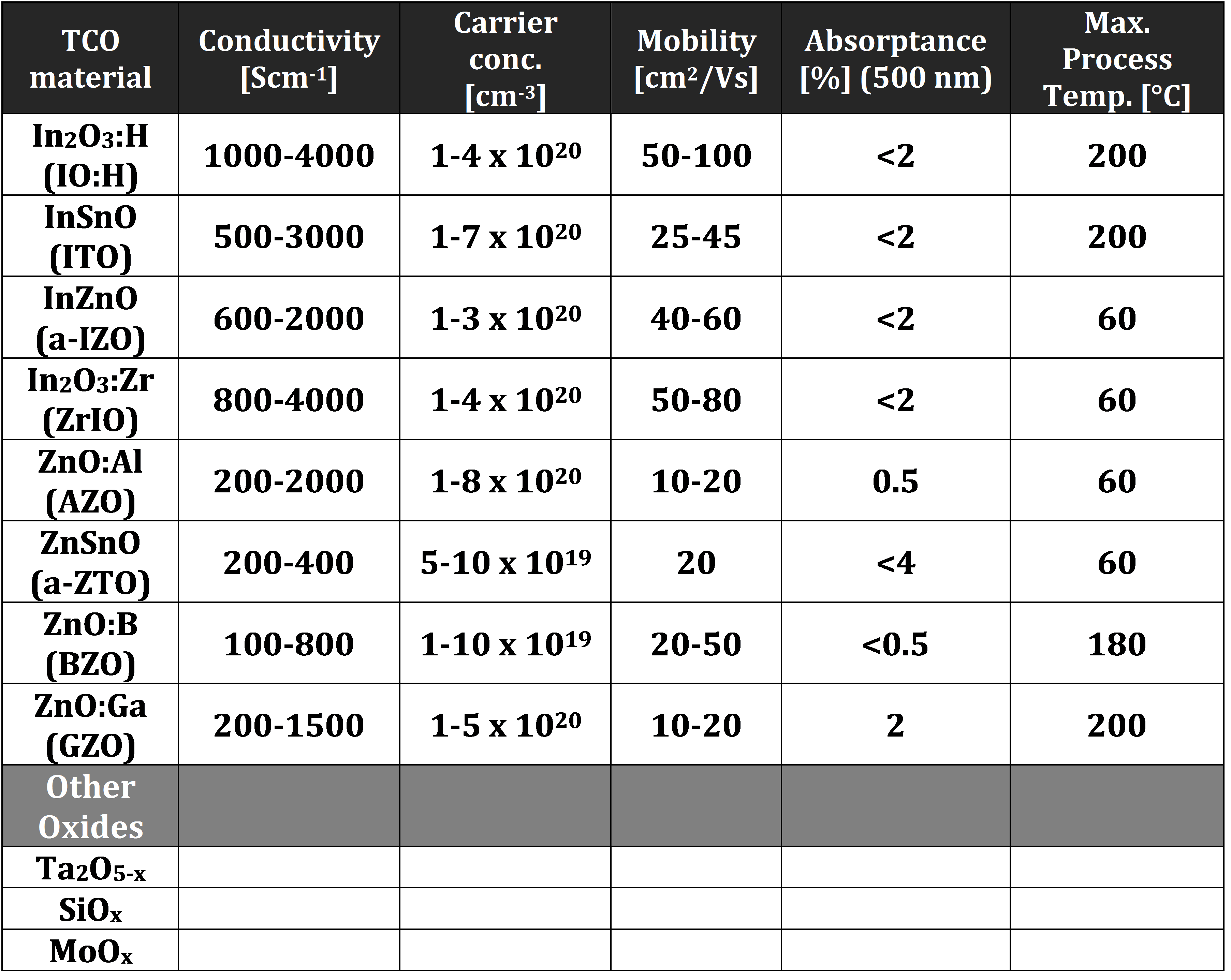
List of available TCOs at PVLab
Deposition and characterization tools
- DC/RF-sputtering
- Low Pressure Chemical Vapor Deposition (CVD)
- Hall effect setup (T-dep)
- UV-Vis-NIR spectrophotometer
- FTIR & Raman spectrometer
- Atomic force microscope
- Profilometer
- Ellipsometer
- TEM/SEM
Key publications:
- E. Rucavado, Q. Jeangros, D. F. Urban, J. Holovský, Z. Remes, M. Duchamp, F. Landucci, Rafal Dunin-Borkowski, W. Körner, C. Elsässer, A. Hessler-Wyser, M. Morales-Masis and C. Ballif, “Enhancing the optoelectronic properties of amorphous zinc-tin oxide by passivation of sub-gap defects: a theoretical and experimental demonstration”, Phys. Rev. B 95, 24 (2017)
- M. Morales-Masis, S. De Wolf, R. Woods-Robinson, J. Ager, C. Ballif, “Transparent Electrodes for Efficient Optoelectronics”, Invited Progress Report, Adv. Electron. Mater. 3, 1600529 (2017)
- L. Fanni, A. Aebersold, M. Morales-Masis, M. Ledinsky, S. Escrig, A. Vetushka, D. Alexander, A. Hessler-Wyser, A. Fejfar, C. Hébert, S. Nicolay, and C. Ballif, “Direct imaging of dopant distribution in polycrystalline ZnO films”, ACS Applied Materials & Interfaces 9, 8 (2017)
- J. Werner, A. Walter, E. Rucavado, S.-J. Moon, D. Sacchetto, M. Rienaecker, R. Peibst, R. Brendel, X. Niquille, S. De Wolf, P. Löper, M. Morales-Masis, S. Nicolay, B. Niesen, C. Ballif, “Zinc Tin Oxide as High-Temperature Stable Recombination Layer for Mesoscopic Perovskite/Silicon Monolithic Tandem Solar Cells”, Appl. Phys. Lett. 109 (2016)
- F. Dauzou, P. C. P. Bouten, A. Dabirian, Y. Leterrier, C. Ballif, M. Morales-Masis, “Mechanical integrity of hybrid indium-free electrodes for flexible devices”, Organic Electronics 35, 136 (2016)
- M. Morales-Masis, F. Dauzou, Q. Jeangros, A. Dabirian, H. Lifka, R. Gierth, M. Ruske, D. Moet, A. Hessler-Wyser, C. Ballif, “An Indium-Free Anode for Large-Area Flexible OLEDs: Defect-Free Transparent Conductive Zinc Tin Oxide”, Adv. Funct. Materials 26, 3 (2016)
- A. Dabirian, A. Lachowicz, J.-W. Schüttauf, B. Paviet-Salomon, M. Morales-Masis, A. Hessler-Wyser, M. Despeisse and C. Ballif, “Metallization of Si heterojunction solar cells by nanosecond laser ablation and Ni-Cu plating”, Solar Energy Materials and Solar Cells 159, 243 (2015)
- A. Dabirian, S. Martin de Nicolas, B. Niesen, A. Hessler-Wyser, S. De Wolf, M. Morales-Masis and C. Ballif, “Tuning the Optoelectronic Properties of ZnO:Al by Addition of Silica for Light Trapping in High-Efficiency Crystalline Si Solar Cells”, Adv. Mater. Interfaces 3, 3 (2015)
- M. Morales-Masis, S. Martin De Nicolas, J. Holovsky, S. De Wolf and C. Ballif, “Low-Temperature High-Mobility Amorphous IZO for Silicon Heterojunction Solar Cells”, IEEE J. of Photovoltaics 5, 5 (2015)
- T. Tohsophon, A. Dabirian, S. De Wolf, M. Morales-Masis and C. Ballif, “Environmental stability of high-mobility indium-oxide based transparent electrodes”, APL Materials 3, 116105 (2015)
- L. Fanni, A. B. Aebersold, M. Morales-Masis, D. T. L. Alexander, A. Hessler-Wyser, S. Nicolay, C. Hébert and C. Ballif, “Increasing Polycrystalline Zinc Oxide Grain Size by Control of Film Preferential Orientation”, Cryst. Growth Des. 15, 12 (2015)