Keywords: flexible solar cells, plastic substrates, light trapping, embossing processes
Background
Thin film silicon solar cells are classified into p-i-n and n-i-p configurations which refer to their deposition sequence; n-i-p processing starts with the n-layer which is normally grown on a metallic back contact. Historically this configuration is connected to flexible substrates because it was used on opaque substrates or poorly transparent substrates like steel foils or high temperature polymers. However, the configuration is not limited to this choice, it is in fact compatible with any kind of substrates, such as rigid or flexible, transparent or opaque. Nevertheless, flexible substrates have remained the main application of n-i-p cells because roll-to-roll processing makes them very interesting to reduce the production costs as well as the energy payback time, particularly when low cost substrates like poly-ethylene are used.
The activities of the n-i-p group combine general aspects of thin film silicon solar cells with special requirements that are imposed by the deposition sequence and the desired compatibility with low temperature substrates. Two main lines of work can be distinguished:
. Substrate texturing
. Light scattering and absorption enhancement
These two combined lines result in, for example, high efficiency triple junctions cell on innovative flat light scattering substrate presented in the last section.
Towards a more fundamental understanding of absorption enhancement in solar cells, we fabricate cells on periodic gratings that permit the study of coupling into guided modes [1].
We obtained fully flexible solar cells on a low cost poly-ethylene substrate with a stabilized efficiency of 9.8% for 0.25cm2 laboratory cells [2].
Research highlights
Substrate texturing
Amorphous and microcrystalline silicon are poor absorbers, particularly for light with energies just above their respective band gaps. Some means of absorption enhancement is required which is commonly called light trapping. It can be achieved by texturing of the interfaces. A common approach for n-i-p cells are back contacts made from so called “hot silver”, which is the texture that silver develops by partial recrystallization during growth on a heated substrate.
Unfortunately this is too hot for poly-ethylene, we have to devise other ways. We investigate the incorporation of texture into the substrate itself, during cell fabrication this texture is carried into the other interfaces because of conformal coverage.
Periodic substrate textures
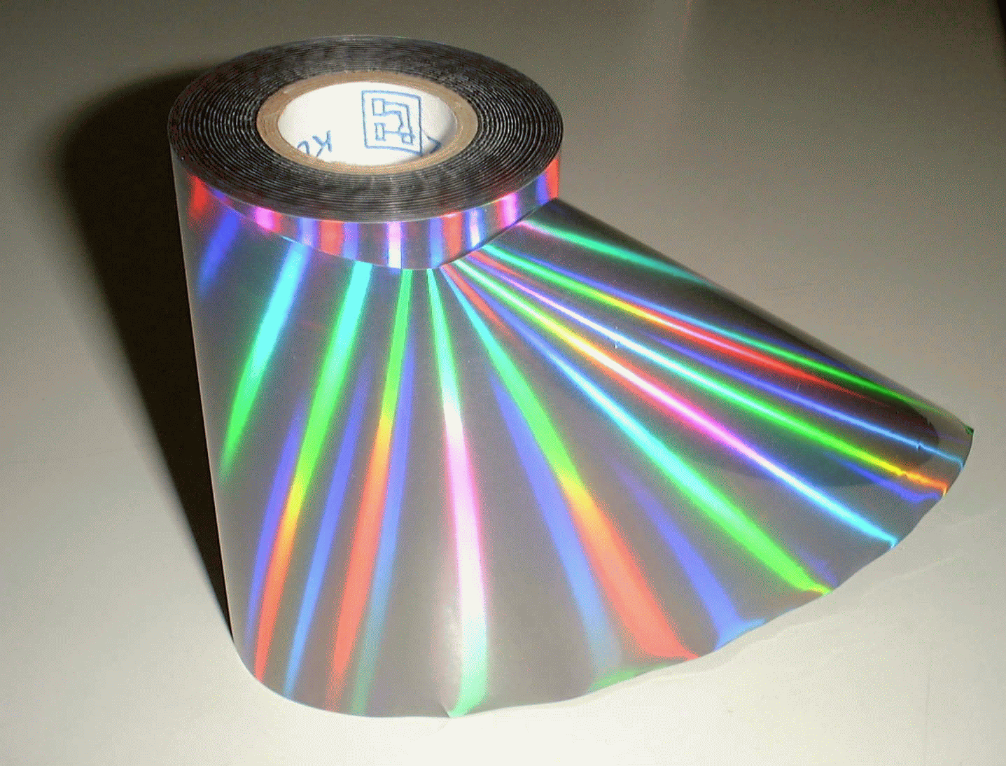
We obtained promising results on low cost poly-ethylene substrates like the one shown below. The substrate texture has been manufactured by a commercial manufacturer.
 |
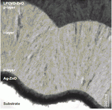 |
The used texture is periodic with a simple sinusoidal wave pattern, thus the incoming light is diffracted into the rainbow colours. For use in solar cells the substrate is coated with back reflector consisting of silver and zinc-oxide. The right figure shows that the back reflector reproduces the substrate texture, but silicon with a thickness comparable to the period already modifies significantly the sinusoidal wave into something that resembles an inverse cycloid.
Embossing
In addition to the substrate shown above, we also investigate embossing processes in order to manufacture novel substrates textures.
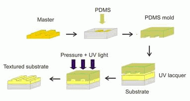 |
The figure above illustrates the embossing process; starting from a master substrate, a negative mold is formed in a polymer (PDMS), then the mold is brought into contact with a UV-sensible lacquer on a substrate. After curing by UV expose it is demolded and the initial texture is reproduced on the substrate.
| |
The process permits, among other options, to reproduce textures that require high temperature processes like hot silver on any other substrate, for example poly-ethylene substrate.
This process reproduces the initial texture with high fidelity. The image above compares AFM surface morphologies of a ZnO master (left) and a replica (right). Features with size below 100 nm are well reproduced.
More information: articles K. Söderström et.al. and J. Escarré et.al.
Light scattering and absorption enhancement
Absorption enhancement in silicon by light scattering at textured interfaces has been proposed as early as 1982 by E. Yablonovitch. The idea is the following; take a slab of silicon with textured surface and shine weakly absorbed light on it. The transmitted light will be scattered at the surface roughness, some of it into angles above the Brewster angle. This part will bounce back and forth within the slab by total internal reflection. It would thus be trapped until its complete absorption, except that each bounce scatters a certain part out of the slab. The amount of light trapping thus depends on the angular width of this so-called escape cone. This can be related to an average light path enhancement of 4 times the square of the refractive index which is about 60 for silicon. There are a few underlying assumptions that are quite difficult to realize. Despite a significant amount of research over the years, the path enhancement in current cells is more likely to be between 20 and 30, and it is still an open question how Yablonovitch’s limit can be reached. Part of the work in the n-i-p group is devoted to the investigation of such fundamental questions, but always keeping in mind the application in real devices.
Plasmons and guided modes
A light beam that bounces back and forth within a slab by total internal reflection is not an unknown concept in optics, in fact this a simplified description of waveguides. An alternate view on light trapping is thus simply the question of how efficient we can couple an incoming plane wave to guided modes in the silicon layer. So far there appears little relation with plasmons, but remember that plasmon polaritons (as they should be called in this context) are just waves that propagate parallel to the interface in a multilayer structure; therefore the title of this section.
 |
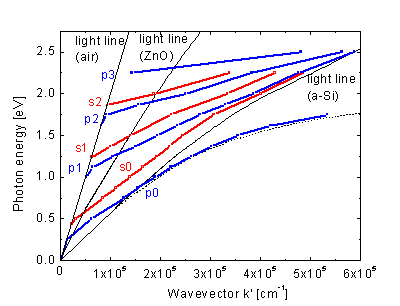 |
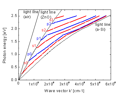
Waveguides are often discussed in terms of dispersion diagrams where the photon energy is plotted against the momentum p (or the wave vector k). For photons these two quantities are related by the speed of light, thus they are represented by straight lines in such a diagram. Note that perpendicular incidence would mean a line that falls on the energy axis. The indicated light lines represent grazing propagation parallel to the interfaces; there is a slight curvature because the refractive index depends on energy.
The diagram to the left shows the modal structure of a 200 nm thick a-Si “waveguide” between air and a zinc-oxide substrate. Such an asymmetric structure is known to have a cut-off, i.e. no guided wave can propagate at energies below 0.25 eV. Between 0.25 and 0.75 eV, only the fundamental mode of s-polarization (s0) can be guided, between 0.75 and 1.25 it can guide two modes (s0 and p0), and for higher energies more and more modes appear. All of these modes are confined between the light lines of silicon and zinc-oxide.
The diagram to the right shows a yet more unusual configuration consisting of a 200 nm thick silicon “waveguide” between a silver “cladding” and air. Most of the modes resemble the waveguide modes of the left image, only that they extend a little further to the left, going as far as the light line of air. Only the lowest energy mode behaves a little strange; it is p-polarized, it has no cut-off, and it runs below the light line of silicon. This particular p0 mode is called plasmon polariton. As mentioned above, it does not propagate in a guiding medium but on the interface between two media.
Light trapping and guided modes
More evidence for the correspondence between light trapping and guided modes was produced in the following experiment: Solar cells were fabricated on a substrate textured with a 1D sinusoidal grating with known period. Such a periodicity folds the above diagrams into Brillouin zones and perpendicular incidence can be represented by vertical lines emerging from the centre of each Brillouin zone. Whenever the characteristics of guided modes and such a vertical line intersects, coupling becomes possible. The excitation of guided modes should thus be visible for specific energies in the form of sharp resonance phenomena. For the 1D grating there should be an additional dependence on the polarization of the incident light.
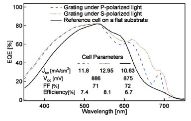 |
The figure shows the external quantum efficiencies of cells on the grating and a flat reference substrate. Note that there are sharp resonances between 600 and 750 nm. The observed polarization dependence and their variation with changes of the angle of incidence further support the idea of guided mode excitation.
High efficiency triple junctions cell on innovative flat light scattering substrate
To reconcile the opposing requirements of layer growth and light scattering which need flat and rough interfaces, respectively, the separation of the light-scattering interface from the growth interface would be of high interest. With this new approach, light scattering is promoted by a textured layer with a low index of refraction filled with a material with a higher refractive index. This stack is then polished to obtain a flat substrate onto which the cell is grown.
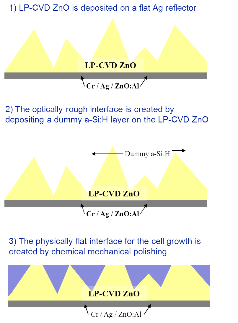
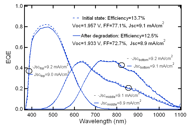
We first fabricated this type of substrate as shown in the figure above and experimentally studied them in single-junction, thick µc-Si:H solar cells [Söderström Solmat 2012]. In second we have been able to fully exploit the potential of these substrates to lead to high efficiency solar cells by growing triple-junctions a-Si:H/µc-Si:H/µc-Si:H in nip configuration. This solar cell exhibits efficiencies of 13.7% in the initial state and 12.5% after degradation as shown in the below. The efficiency after degradation is among the highest reported to this date for purely silicon based n-i-p thin film solar cells [Söderström accepted for publication in JAP].
Key publications
| [1] | K. Söderström, G. Bugnon, F.-J. Haug, S. Nicolay and C. Ballif, Experimental study of flat light-scattering substrates in thin-film silicon solar cells, Solar Energy Materials and Solar Cells, vol. 101, p. 193-199, Elsevier, 2012 |
| [2] | K. Söderström, F.-J. Haug, J. Escarré, O. Cubero, C. Ballif, Photocurrent increase in n-i-p thin film silicon solar cells by guided mode excitation via grating coupler, Applied Physics Letters 96, 213508, 2010 |
| [3] | T. Söderström, F.-J. Haug, X. Niquille, V. Terrazzoni, and C. Ballif, Asymmetric intermediate reflector for tandem micromorph thin film silicon solar cells, Appl. Phys. Lett., Vol 94 , pp. -063501, 2009 |
| [4] | F.-J. Haug, T. Söderström, O. Cubero, V. Terrazzoni-Daudrix, X. Niquille, S. Perregeaux, and C. Ballif, Periodic textures for enhanced current in thin film silicon solar cells, Presented at the MRS Spring Meeting, San Francisco, 2008 |
| [5] | T. Söderström, F.-J. Haug, V. Terrazzoni-Daudrix, X. Niquille, M. Python and C. Ballif, N/I buffer layer for substrate microcrystalline thin film silicon solar cell, Journal of Applied Physics, Vol 104, pp. -104505, 2008 |