Perovskite Cells for Tandem Applications
|
Group members:
|
Dr. Q. Jeangros, Dr. M. Bräuninger, Dr. T.C.J. Yang, J. Werner, F. Sahli, P. Fiala
|
|
Running projects:
|
Synergy (Nano-Tera.ch, SFOE), PV2050 (SNF), EPISODE (SNF), CHEOPS (H2020), POSITS (H2020-MSCA-IF-2016)
|
Keywords: perovskite solar cell, tandem, monolithic, 4-terminal, semi-transparent
Background
Metal halide perovskite solar cells have recently made tremendous progress, with record efficiencies beyond 20%. Interestingly, perovskite cells are not only very efficient, but also have a high and tunable band gap. This, together with the fact that they can be fabricated with cheap processing techniques, makes them highly interesting for application in tandem cells. In such a tandem device, the perovskite cell acts as the top cell, absorbing the visible light, while a solar cell with a narrow band gap acts as the bottom cell and harvests photons in the near-infrared part of the solar spectrum (Figure 1). Silicon solar cells, which reach efficiencies of up to 25.6% and dominate the global photovoltaics market, are the most attractive candidates for bottom cells. As this silicon cell efficiency record is already very close to the practical efficiency limit of this type of solar cells, perovskite/silicon tandem cells with their potential for ultra-high efficiencies at affordable costs represent the most straight forward way to decrease the overall cost of photovoltaic systems and consequently also to reduce the price of electricity for end-users.
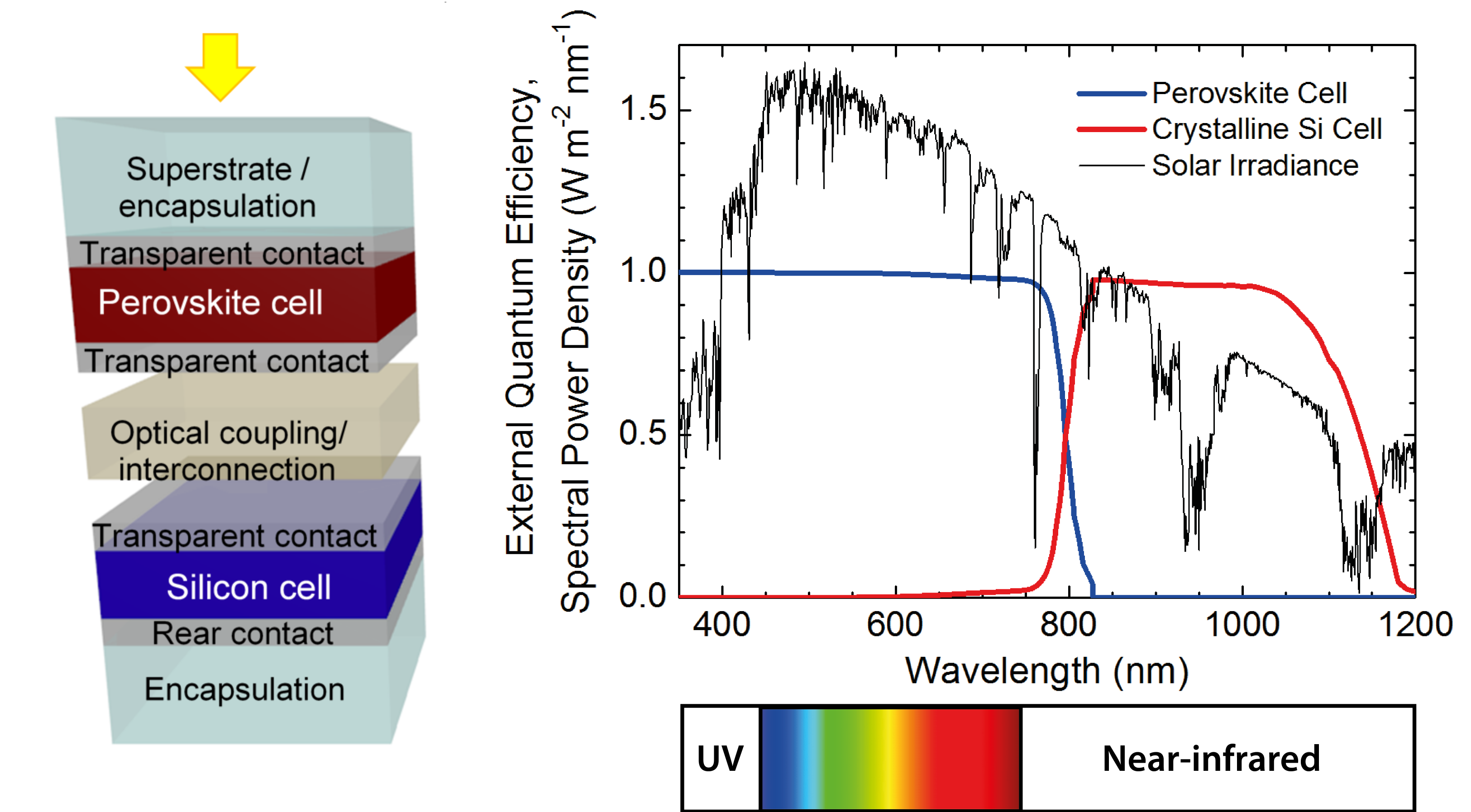
Figure 1. Left: Schematic illustration of a perovskite/silicon tandem cell. Right: Light enters through the perovskite cell, where mostly the visible part of the solar spectrum is absorbed. Near-infrared light is transmitted to the silicon cell where it is absorbed.
Research highlights
Band edge and sub-band gap absorption of perovskite layers
For application in perovskite/silicon tandem cells, the perovskite absorber layer has to be highly transparent at photon energies below its band gap. Any light absorbed in this sub-bandgap wavelength range would neither contribute to the photocurrent of the perovskite cell nor be transmitted to the silicon bottom cell, and therefore would severely limit performance. In collaboration with the Czech Academy of Sciences, we conducted highly sensitive photothermal deflection spectroscopy and Fourier-transform photocurrent spectroscopy to investigate absorption near and below the perovskite band edge [12]. The absorption edge (Figure 2) of the CH3NH3PbI3 perovskite material was found to be very steep, with no observable sub-band gap absorption. The lack of sub-band gap absorption confirms that perovskites are suitable for tandem cells. By further analyzing the absorption edge, an Urbach energy of as low as 15 meV was obtained, confirming the excellent electronic of the perovskite material.
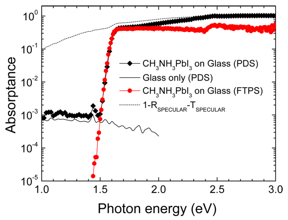
Figure 2. Absorptance spectra of a CH3NH3PbI3 perovskite layer obtained by photothermal deflection spectroscopy (PDS) and Fourier-transform photocurrent spectroscopy (FTPS). Figure published by S. de Wolf et al. in J. Phys. Chem. Lett. 5, 1035 (2014).
Perovskite cells with transparent front and rear electrodes
The rear contact of a perovskite solar cell is typically opaque, using an evaporated metal such as Au, Ag or Al. However, for the application in tandem cells, a perovskite cell with a transparent rear electrode is required. This is a challenging task as this electrode has to be deposited on top of the complete cell stack, including sensitive transport layers and the perovskite layer. At PV-Lab, in collaboration with CSEM, a transparent electrode based on sputtered transparent oxides has been developed (Figure 3). By inserting a thin metal oxide buffer layer to mitigate sputter damage, device efficiencies of up to 10.7% were reached for perovskite cells with an average transmittance of more than 60% in the 800–1200 nm wavelength range [6, 9]. By further improving light out-coupling and replacing the FTO electrode with a more transparent one based on ITO, the transparency in this wavelength range was improved to more than 70%.
Figure 3. Top: Scanning electron microscopy image and schematic illustration of a perovskite cell with transparent front and rear electrodes based on transparent conductive oxides. To mitigate damage induced during the deposition of the indium zinc oxide (IZO) rear electrode, a thin molybdenum oxide layer was deposited onto the spiro-OMeTAD hole transport layer. Bottom: Current density-voltage curves and external quantum efficiency of cells with different rear electrodes. Picture published by J. Werner et al. in Sol. Energy Mater. Sol. Cell. 141, 407 (2015).
4-Terminal tandem cells
Using a perovskite solar cell with two transparent electrodes, mechanically stacked 4-terminal tandem devices with efficiencies of up to 19.6% were made (Figure 4) [6]. These tandems used silicon bottom cells made by the a-Si/c-Si Heterojunction Solar Cell group. By further optimization, efficiencies of up to 20.6% were reached, which is beyond the performance of each sub cell. However, the external quantum efficiency spectra in Figure 3 clearly show that parasitic absorption in the perovskite cell and reflection at the various surfaces of the tandem cell limit the silicon bottom current. The reduction of these optical losses is crucial to further optimize tandem cell performance.
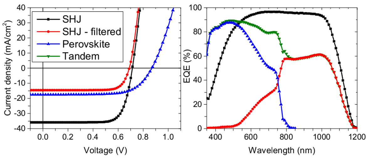
Figure 4. Current density-voltage curves (left) and external quantum efficiency spectra (EQE, right) of a silicon heterojunction cell, either measured as a single-junction solar cell or illuminated through a perovskite top cell with a transparent rear electrode. The current density-voltage curve and EQE spectrum of the perovskite cell are also shown for comparison. Picture published by J. Werner et al. in Sol. Energy Mater. Sol. Cell. 141, 407 (2015).
Efficiency potential of perovskite/Si tandem cells
To reach efficiencies beyond the single-junction limit, tandem devices have to be highly optimized, especially regarding current distribution between the two sub cells and the reduction of parasitic absorption losses. There are several approaches to estimate the efficiency potential of tandem cells:
In a first step, an upper limit for the efficiency can be given by assuming no parasitic absorption losses and ideal contacts. For a tandem using a CH3NH3PbI3-based top cell and an silicon heterojunction bottom cell, this efficiency limit equals ~35-37%, depending on whether light trapping schemes are employed in the top cell or not [11].
A more realistic approach involves the detailed assessment of all the loss mechanisms present in a tandem cell, starting from the efficiency of the actual device and estimating its efficiency potential if all loss mechanisms could be removed. Using this approach, an efficiency limit of 31.6% was estimated for 4-terminal CH3NH3PbI3/silicon tandem cells [9]. This loss analysis also allows for the identification of the most critical limiting factors. For example, with state-of-the-art perovskite and silicon heterojunction cells, but without eliminating parasitic absorption typically occurring in the hole transport layer and the transparent electrodes, the tandem efficiency is limited to ~19%, which is far below that of the silicon bottom cell. However, if all parasitic absorption could be removed, for example by using a hole conductor-free perovskite cell and fully transparent contacts, an efficiency of 27.6% could be reached. These results emphasize the importance of eliminating parasitic absorption in tandem devices. In addition, the performance can be further improved to >31% by current matching between the two sub cells.
A more realistic approach involves the detailed assessment of all the loss mechanisms present in a tandem cell, starting from the efficiency of the actual device and estimating its efficiency potential if all loss mechanisms could be removed. Using this approach, an efficiency limit of 31.6% was estimated for 4-terminal CH3NH3PbI3/silicon tandem cells [9]. This loss analysis also allows for the identification of the most critical limiting factors. For example, with state-of-the-art perovskite and silicon heterojunction cells, but without eliminating parasitic absorption typically occurring in the hole transport layer and the transparent electrodes, the tandem efficiency is limited to ~19%, which is far below that of the silicon bottom cell. However, if all parasitic absorption could be removed, for example by using a hole conductor-free perovskite cell and fully transparent contacts, an efficiency of 27.6% could be reached. These results emphasize the importance of eliminating parasitic absorption in tandem devices. In addition, the performance can be further improved to >31% by current matching between the two sub cells.
Finally, numerical simulations are a powerful tool to estimate efficiency potentials and provide guidelines for the choice of materials and layer thicknesses. In collaboration with the University of Ljubljana (Laboratory of Photovoltaics and Optoelectronics, directed by Prof. M. Topič), monolithic and 4-terminal perovskite/silicon tandem cells were simulated, both with textured and planar silicon cells (Figure 5) [7]. These simulations were based on the experimentally measured refractive indices of all materials present in the tandem devices [10]. As a main conclusion from this study, it was found that the commonly used hole transport material spiro-OMeTAD has to be replaced by a more transparent material in monolithic tandem cells to reach efficiencies beyond the single-junction silicon cell record value of 25.6%. In addition, comparing textured and flat cells, it was found that the presence of perovskite cell may strongly reduce reflection losses and therefore enable efficient non-textured perovskite/silicon tandem cells.
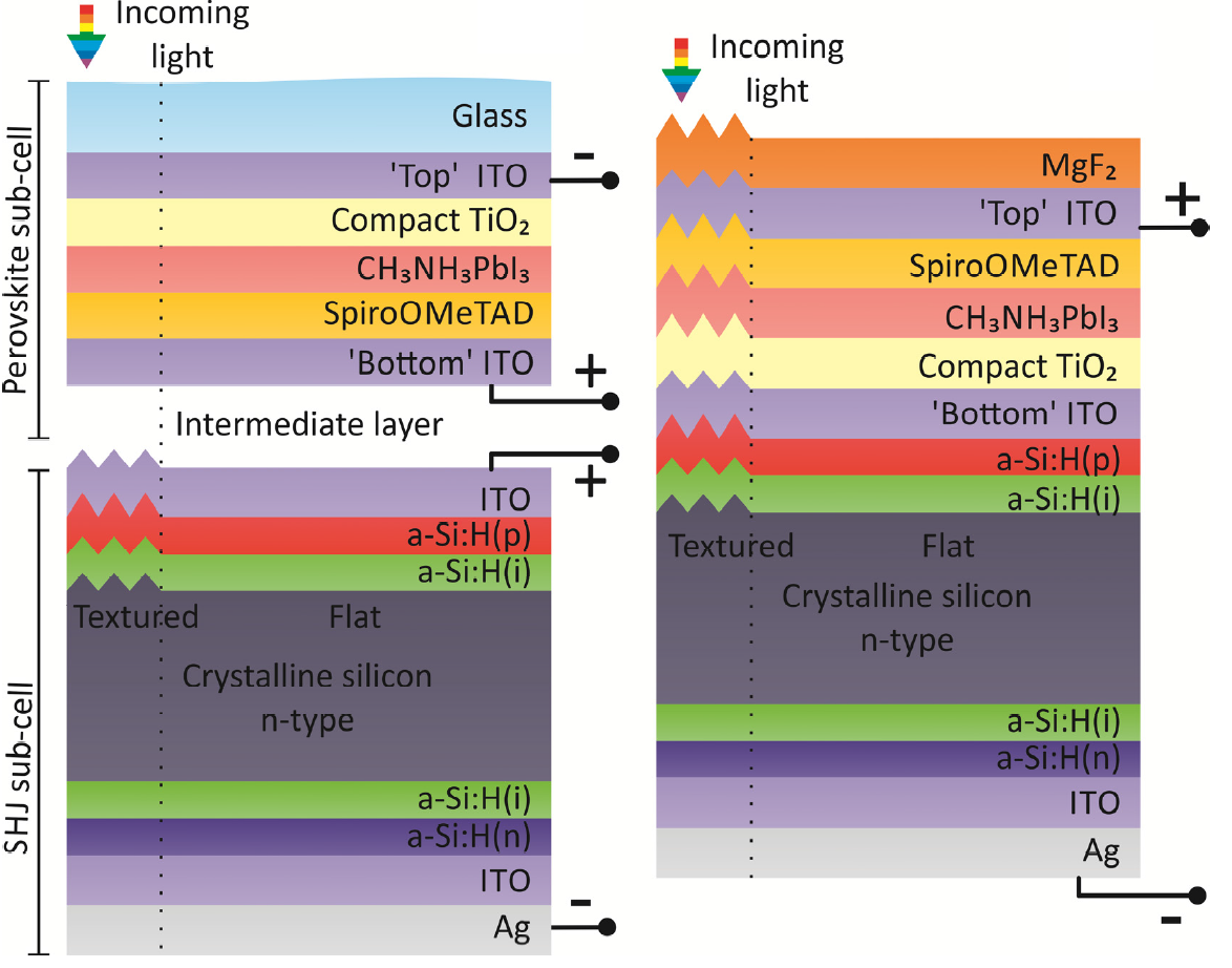
Figure 5. Schematic illustration of simulated perovskite/silicon heterojunction tandem cells. Picture published by M. Filipič et al. in Opt. Express 23 (7), A263 (2015).
Mixed halide perovskites
With a band gap of ~1.55 eV the CH3NH3PbI3 material is not ideal to reach maximal efficiencies in monolithic tandem devices with a silicon bottom cell. Highest efficiencies would be expected for perovskite band gaps of 1.7-1.8 eV. By adding bromine into the perovskite material, the band gap can be tuned to higher energies, this making it more suitable for tandem applications. However, processing of such mixed halide materials has been shown to be challenging, often resulting in inhomogeneous layer formation. In collaboration with the Czech Academy of Sciences, we performed micro-Raman spectroscopy on Br/I mixed halide layers and found a simple method to directly observe phase separation as well as to quantify with high spatial resolution the Br/I ratio (Figure 6) [8].
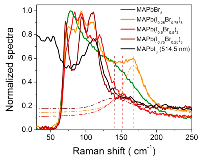
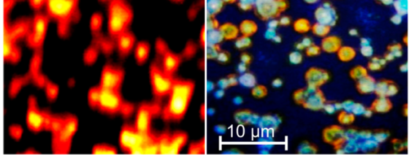
Figure 6. Top: Raman shift spectra for mixed halide perovskite layers with several Br/I ratios. Bottom: Micro-Raman map (left) and microscopy image (right) of Br/I mixed halide perovskite layer. Picture published by M. Ledinsky et al. in J. Phys. Chem. Lett. 6, 401 (2015).
Key publications:
| [1] |
J. Werner, B. Niesen, and C. Ballif, Perovskite/Silicon Tandem Solar Cells: Marriage of Convenience or True Love Story? – An Overview, Adv. Mater. Interfaces, 1700731, 2017
|
| [2] |
F. Sahli, B. A. Kamino, J. Werner, M. Bräuninger, B. Paviet-Salomon, L. Barraud, R. Monnard, J. P. Seif, A. Tomasi, Q. Jeangros, A. Hessler-Wyser, S. De Wolf, M. Despeisse, S. Nicolay, B. Niesen, C. Ballif, Improved Optics in Monolithic Perovskite/Silicon Tandem Solar Cells with a Nanocrystalline Silicon Recombination Junction, Adv. Energy Mater., 1701609, pp. 1–8, 2017
|
|
[3]
|
J. Werner, L. Barraud, A. Walter, M. Bräuninger, F. Sahli, D. Sacchetto, N. Tétreault, B. Paviet-Salomon, S.-J. Moon, C. Allebé, M. Despeisse, S. Nicolay, S. De Wolf, B. Niesen, C. Ballif, Efficient Near-Infrared-Transparent Perovskite Solar Cells Enabling Direct Comparison of 4-Terminal and Monolithic Perovskite/Silicon Tandem Cells, ACS Energy Lett. 1, 474-480 (2016).
|
|
[4]
|
J. Werner, J. Geissbühler, A. Dabirian, S. Nicolay, M. Morales-Masis, S. De Wolf, B. Niesen, C. Ballif, Parasitic Absorption Reduction in Metal Oxide-Based Transparent Electrodes: Application in Perovskite Solar Cells, ACS Appl. Mater. Interf. 8, 17260-17267 (2016).
|
|
[5]
|
J. Werner, C.-H. Weng, A. Walter, L. Fesquet, J. P. Seif, S. De Wolf, B. Niesen, C. Ballif, Efficient Monolithic Perovskite/Silicon Tandem Solar Cell With Cell Area > 1 cm2, J. Phys. Chem. Lett. 7, 161-166 (2016).
|
|
[6]
|
J. Werner, G. Dubuis, A. Walter, P. Löper and S.-J. Moon, S. Nicolay, M. Morales-Masis, S. De Wolf, B. Niesen, C. Ballif, Sputtered rear electrode with broadband transparency for perovskite solar cells, Sol. Energy Mater. Sol. Cell. 141, 407 (2015).
|
|
[7]
|
M. Filipič, P. Löper, B. Niesen, S. De Wolf, J. Krč, C. Ballif, M. Topič, CH3NH3PbI3 perovskite/silicon tandem solar cells: characterization based optical simulations, Opt. Express 23 (7), A263 (2015).
|
|
[8]
|
M. Ledinsky, P. Löper, B. Niesen, J. Holovsky, S.-J. Moon, J.-H. Yum, S. De Wolf, A. Fejfar, C. Ballif, Raman Spectroscopy of Organic-Inorganic Halide Perovskites, J. Phys. Chem. Lett. 6, 401 (2015).
|
|
[9]
|
P. Löper, S.-J. Moon, S. Martín de Nicolas, B. Niesen, M. Ledinsky, S. Nicolay, J. Bailat, J.-H. Yum, S. De Wolf, C. Ballif, Organic–inorganic halide perovskite/crystalline silicon four-terminal tandem solar cells, Phys. Chem. Chem. Phys. 17, 1619 (2015).
|
|
[10]
|
P. Löper, M. Stuckelberger, B. Niesen, J. Werner, M. Filipič, S.-J. Moon, J.-H. Yum, M. Topič, S. De Wolf, C. Ballif, Complex Refractive Index Spectra of CH3NH3PbI3 Perovskite Thin Films Determined by Spectroscopic Ellipsometry and Spectrophotometry, J. Phys. Chem. Lett. 6, 66 (2014).
|
|
[11]
|
P. Löper, B. Niesen, S.-J. Moon, S. Martin de Nicolas, J. Holovsky, Z. Remes, M. Ledinsky, F.-J. Haug, J.-H. Yum, S. De Wolf, C. Ballif, Organic–Inorganic Halide Perovskites: Perspectives for Silicon-Based Tandem Solar Cells, IEEE J. Photovolt. 4, 1545 (2014).
|
|
[12]
|
S. De Wolf, J. Holovsky, S.-J. Moon, P. Löper, B. Niesen, M. Ledinsky, F.-J. Haug, J.-H. Yum, C. Ballif, Organometallic halide perovskites: sharp optical absorption edge and its relation to photovoltaic performance, J. Phys. Chem. Lett. 5, 1035 (2014).
|